
Intel Shows Off Glass Substrate Packaging for Next-Gen Chips
Introduction
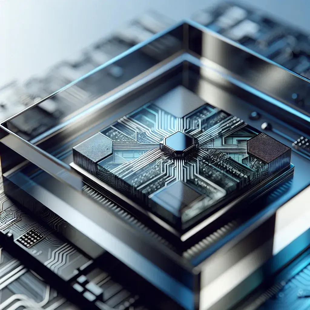
In recent years, the semiconductor industry has witnessed rapid advancements, driven by the ever-increasing demand for processing power and efficiency. One of the most significant developments comes from Intel, a leading name in the tech world. Intel has recently unveiled its groundbreaking glass substrate packaging technology designed for next-generation chips. This innovation not only promises to enhance performance but also addresses the challenges posed by traditional materials. In this article, we will explore the implications of Intel’s glass substrate packaging, its benefits, and what it means for the future of computing.
The Significance of Glass Substrate Packaging
Intel’s introduction of glass substrate packaging marks a pivotal shift in semiconductor manufacturing. Traditionally, silicon has been the primary material used for chip substrates. However, as chips become more complex and miniaturized, the limitations of silicon are increasingly apparent. Glass, on the other hand, offers several advantages:
- Enhanced Electrical Performance: Glass substrates allow for better electrical performance due to their lower dielectric constant compared to silicon.
- Lower Weight: Glass is significantly lighter than silicon, which reduces the overall weight of electronic devices.
- Improved Thermal Stability: Glass substrates can withstand higher temperatures, making them suitable for high-performance applications.
- Increased Density: The use of glass enables higher integration density, allowing for more transistors to be packed into a smaller area.
Historical Context
To fully appreciate the significance of Intel’s glass substrate packaging, it’s essential to understand its historical context. The semiconductor industry has evolved significantly since the invention of the first integrated circuits in the 1960s. Early chips were made from discrete components and large ceramic packages. As technology advanced, manufacturers began using silicon wafers, which provided a more efficient way to produce complex circuits.
However, as the demand for smaller, faster, and more efficient chips grew, the limitations of silicon became evident. Issues such as heat dissipation, electrical performance, and size constraints prompted researchers to explore alternative materials. The move towards glass substrates is a culmination of decades of research and development aimed at overcoming these challenges.
Future Predictions: The Path Forward
Looking ahead, the adoption of glass substrate packaging has the potential to redefine the semiconductor landscape. As technology continues to evolve, several predictions can be made regarding its impact:
- Wider Adoption Across Industries: As the benefits of glass substrates become more apparent, industries ranging from consumer electronics to automotive will likely adopt this technology.
- Increased Performance Metrics: Future chips utilizing glass substrates are expected to achieve significant performance improvements, particularly in high-demand applications such as artificial intelligence and machine learning.
- New Applications: The improved capabilities of chips with glass substrates may lead to entirely new applications and innovations we cannot yet envision.
Pros and Cons of Glass Substrate Packaging
Pros
- Higher Performance: The electrical properties of glass allow for faster signal transmission and reduced power consumption.
- Scalability: Glass substrates can be manufactured in larger sizes, making it easier to scale production for various applications.
- Durability: The thermal and mechanical stability of glass enhances the longevity and reliability of chips.
Cons
- Manufacturing Challenges: The production process for glass substrates is more complex than traditional silicon substrates, which may result in higher costs initially.
- Limited Knowledge Base: As this is a relatively new technology, there may be a learning curve for manufacturers and engineers.
Real-World Examples and Cultural Relevance
The announcement of Intel’s glass substrate packaging has already begun to influence various sectors, particularly in consumer electronics. Companies that rely on high-performance chips, such as gaming and graphics industries, are keenly interested in this innovation. For instance, gaming consoles and high-end graphics cards could benefit immensely from the enhanced capabilities of glass-packaged chips.
Expert Insights
Leading experts in the semiconductor field have expressed excitement about Intel’s new technology. Dr. Lisa Su, CEO of AMD, stated, “The introduction of glass substrate packaging by Intel reflects the ongoing evolution of semiconductor technology. As we push the boundaries of performance, innovations like this will play a crucial role in shaping the future of computing.”
Conclusion
Intel’s unveiling of glass substrate packaging for next-generation chips is a game-changer for the semiconductor industry. By addressing the limitations of traditional silicon substrates, this technology paves the way for faster, more efficient, and more powerful chips. As we look to the future, the implications of this innovation will undoubtedly resonate across various sectors, driving advancements in technology and enhancing our everyday lives. The journey of glass substrates is just beginning, and it promises to be an exciting chapter in the evolution of semiconductor technology.